

 en
 zh
 it
 es
 ja
 sv
 no
 nl
 ko
 fi
 ru
 fr
 de
Third-Generation Solar Cell Technology
Integrated Solar Solutions for Curved Buildings & Outdoor Portable Power


Integrated Solar Solutions for Curved Buildings & Outdoor Portable Power
A quick tour of the material behind every SunFlex module — what it is, why it's different, and why it's ready now.
Perovskite is a crystal structure — ABX₃ — coated as a film thinner than a hair. It isn't a better silicon panel. It's the third generation of solar.
Tap any atom to explore its role →
Large cations sit at the cube's corners. They don't catch light themselves — they hold the lattice in shape. Blending them is how efficiency is traded off against heat and humidity stability.
The metal sits at the center of every [BX₆] octahedron. Its orbitals form the band edges — this is where a photon becomes an electron. All the electrical work happens here.
Six halides bridge neighboring B atoms into a 3D network. Swap iodide for bromide and the band gap shifts — retuning the absorption edge, the color and the voltage. That tunability is unique to perovskites.
A perovskite cell is a stack of five ultra-thin films: conductive – functional – perovskite – functional – conductive. The perovskite layer in the middle makes the charge; the two functional layers sort it; the two conductive layers carry it out.
Tap any layer to see its job →
The front electrode. Transparent so sunlight passes through, yet conductive enough to collect the current every layer underneath produces.
A charge-transport film between the electrode and the perovskite. It guides one type of charge carrier through while blocking the other — that's how electrons and holes get sorted instead of recombining.
The only layer that turns light into electricity. ABX₃ crystals coated as a film under 1 µm thick — photons in, electrons out. Every other layer exists to move or extract that charge.
The matching transport film on the other side of the perovskite. It passes the opposite charge carrier from layer 02, completing the split so both types flow out to different electrodes.
The back electrode. It collects the charges routed down through the stack and sends them around the external circuit — closing the loop that powers your device.
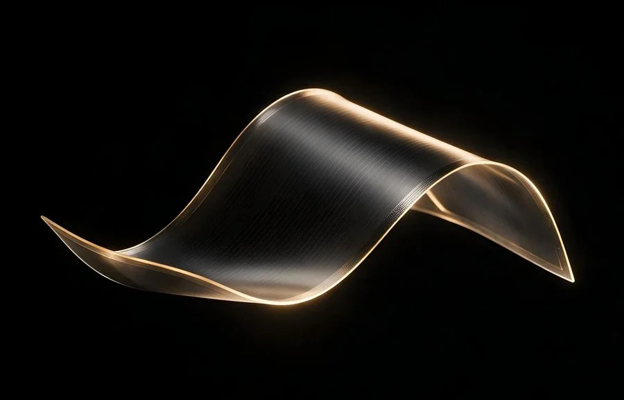
Three generations, one direction: from rigid wafers to printable films. Generation three is what SunFlex makes.
Schematic — not to scale. Thickness of the active light-absorbing layer.
The layer that makes power is thinner than a human hair — coated, not cut. That's why it can bend, weigh almost nothing, and take any shape.
The science took 16 years. The supply chain took a gigafactory. Both are here now — certified, designed for real products, shipping at scale.
Now that you know the material — scroll on and meet the products.

